
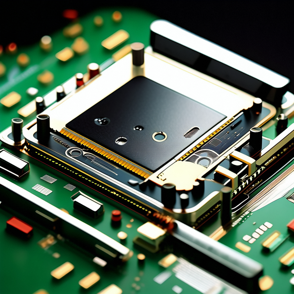
As the core component of modern electronic equipment, the performance and reliability of Integrated Circuit (IC) directly affect the functional performance of the entire electronic system. From smartphones to high-performance computing systems, from automotive electronics to medical devices, IC applications are almost everywhere. However, simply having a high-performance chip is not enough to ensure the success of electronic products, chips need to be connected to the outside world in a stable and reliable way. This brings us to the topic we are going to discuss today – IC packaging technology.
Packaging not only protects the fragile chip from physical damage and environmental factors, but also provides the necessary electrical interfaces that allow the chip to work together with other electronic components. Next, we will delve into the types of IC packaging technologies, considerations, and future trends.
What is IC packaging technology?
In the electronics industry, Integrated Circuit (IC) is one of the core components that make up modern electronic equipment. However, even the most advanced chips need a way to connect with the outside world. This is where IC packaging technology comes into play.
In a nutshell, IC packaging technology refers to the process of securing the chip (Die) inside a package housing and connecting it to an external circuit via pins, solder balls, or other forms of connectors. The package not only provides the necessary electrical interface, but also protects the chip from physical damage and environmental factors, ensuring that the chip can operate stably and reliably in a variety of application environments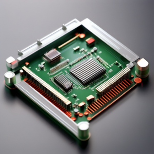
Type of IC package
IC packaging technology can be divided into many types according to different standards, and each type of packaging has its unique characteristics and application scenarios. The following are several common IC package types:
1. Through-Hole Technology (THT)
Definition: One of the earliest forms of packaging, secured by inserting pins through holes in a printed circuit board and welding them.
Advantages: Easy to install and maintain, high reliability.
Disadvantages: large volume, not suitable for high-density assembly.
2. Dual In-line Package (DIP)
Definition: A through-hole technology package with pins arranged in two rows.
Application: Suitable for early digital logic chips and microprocessors.
3. Surface Mount Technology (SMT)
Definition: The basis of modern packaging technology, the package is mounted directly on the surface of the printed circuit board.
Advantages: Small size, suitable for high-density assembly.
Disadvantages: The welding process is demanding and not easy to repair.
4. Ball Grid Array (BGA)
Definition: A form of package with the bottom covered with solder balls, suitable for high-density, high-performance chips.
Advantages: small package area, excellent electrical performance.
Disadvantages: high installation difficulty, complex maintenance.
5. Quad Flat No-Lead (QFN)
Definition: The pins are located on the edge of the package without exposed pins.
Advantages: compact size, good thermal performance.
Disadvantages: Small pin spacing, strict welding requirements.
6. Flip Chip package
Definition: The chip is flipped directly and attached to a pad on the substrate.
Advantages: Short distance signal transmission, reduce signal attenuation.
Disadvantages: high cost and complex process.
7. System in Package (SiP)
Definition: To integrate multiple chips and passive components in a single package.
Advantages: Space saving, simplified design.
Disadvantages: May increase the complexity and cost of packaging.
8. Fan-Out Wafer Level Packaging (FO-WLP)
Definition: A fan-shaped pin layout is formed around the chip.
Advantages: Increase the number of I/O, reduce signal interference.
Disadvantages: The process is difficult and the cost is relatively high.
IC packaging technology precautions
Choosing the right IC packaging technology is critical to ensuring the performance and reliability of electronic products. When designing and selecting a package, there are several key factors to pay special attention to:
1. Thermal management
Consideration: The chip will generate heat during the working process, so it is necessary to choose packaging materials and structures with good heat dissipation performance.
Solution: Use substrate materials with good thermal conductivity, such as copper columns, graphene, etc., and efficient heat sinks or heat pipes.
2. Electrical performance
Consideration: The package should minimize attenuation and reflection during signal transmission to avoid electromagnetic interference (EMI).
Solution: Optimize the pin layout and use Low dielectric constant (low-K) materials to reduce the capacitance effect of the signal path.
3. Mechanical strength
Consideration: The package needs to withstand a certain amount of mechanical stress without damaging the chip.
The solution: Durable packaging materials, such as enhanced epoxy or ceramics, and well-designed packaging structures.
4. Cost effectiveness
Consideration: The cost of packaging is an important part of the total cost, and a balance must be found between performance and cost.
Solution: Evaluate the cost-benefit ratio of different packaging technologies and select the packaging solution that best suits the application needs.
5. Environmental adaptability
Consideration: The package needs to be able to withstand a variety of environmental conditions, such as temperature changes, humidity, etc.
Solution: Use high temperature and moisture resistant packaging materials to ensure that the package will work in harsh environments.
6. Size and weight
Considerations: In portable devices and space-constrained applications, package size and weight are particularly important.
Solution: High-density packaging technologies such as fan-out package (FO-WLP) and Flip Chip are used to reduce package size.
7. Compatibility
Considerations: Packages need to be compatible with existing manufacturing processes and other components.
Solution: Select the type of package that is mature and widely used in the market to ensure smooth production process.
8. Testability
Considerations: Package design should be easy to test to ensure product quality.
Solution: Design easy access test points with easy disassembly and replacement design for easy troubleshooting.
9. Maintainability
Considerations: The package should be easy to maintain and replace, especially in complex systems.
Solution: Modular design for easy on-site repair or replacement.
10. Environmental protection
Consideration: With the increasing demand for sustainable development, the selection of packaging materials needs to consider its environmental characteristics.
Solution: Reduce environmental impact by using recyclable or biodegradable packaging materials.
Future development trend of IC packaging technology
As electronics continue to evolve, IC packaging technology continues to evolve to meet higher performance requirements, smaller sizes, and lower costs. Here are some future trends for IC packaging technology:
1. High-density packaging
Trends: As chip capabilities increase, packaging technologies need to support more I/O interfaces and higher signal density.
Technology: Using Fan-Out Wafer Level Packaging (FO-WLP), Flip Chip, System in Package (SiP) and other technologies.
2. Three-dimensional packaging
Trend: Stacking chips to reduce package size and improve integration.
Technology: Through Silicon Via (TSV) technology to achieve vertical interconnection and three-dimensional stacked packaging.
3. Micro and nano technology
Trend: Using micro and nano technology to improve packaging accuracy and performance.
Technology: Micro and nano manufacturing technology is applied to the precision machining of the package structure to improve the efficiency of signal transmission.
4. Customized packaging
Trend: To provide customized packaging solutions according to different application requirements.
Technology: Use rapid prototyping technology to flexibly adjust package design to suit specific application requirements.
5. Package as System (PAS)
Trend: The deep integration of packaging technology and system design, packaging has become a part of system design.
Technology: Through advanced packaging technology to achieve complex system functions within the package, such as radio frequency (RF) functions, analog functions, etc.
conclusion
As a bridge connecting chips with the outside world, IC packaging technology plays a crucial role in modern electronic devices. With the rapid development of semiconductor technology, packaging technology continues to advance to meet the needs of higher performance, smaller size and lower power consumption. From traditional through-hole technology to modern surface mount technology, to advanced technologies such as high-density packaging and three-dimensional packaging, the development of packaging technology has always been closely related to the needs of the electronics industry. In the future, with the further integration of micro and nano technology, new material science and intelligent technology, IC packaging technology will continue to develop in the direction of higher integration, better thermal management performance and more environmental protection.
TDT-ELE is committed to providing the most cutting-edge IC packaging solutions. Whether it is high performance computing chips or micro packaging needs for consumer electronics, we are able to provide professional service and support. If you are looking for a partner who can help you achieve product innovation, our company will be the ideal choice for you.