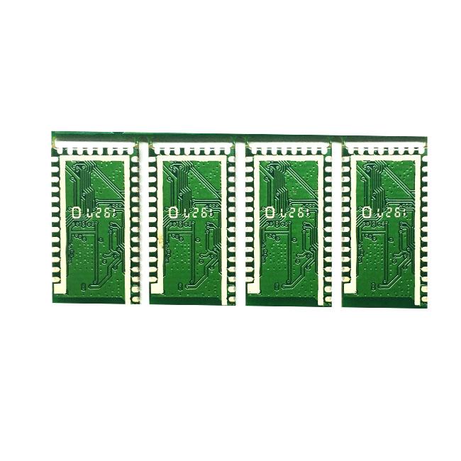
HDI PCB
HDI PCB | |
HDI PCB is characterized by high-density features, including laser micro vias, fine lines, and high-performance thin materials. This increased density can support more functions per unit area. because of its higher circuit density than normal PCBs, the design of HDI PCB can incorporate finer lines and spacing, smaller through holes and pads, and higher connection with pad density. HDI PCBs have blind vias and buried vias, and generally contain micro vias with a diameter of 0.006 or less. | |
PCB circuit board Files format: | Gerber, .pcb, .pcbdoc or .cam |
Printed circuit board Materical: | FR4 standard Tg 140°C,FR4 High Tg 170°C, FR4 and Rogers combined lamination |
PCB board Surface Finishing: | ENIG/OSP/Gold Plating(Soft/hard) /HASL/Imm. Silver/IMM.Tin/Tin Plating/Carbon Ink/Selective /Imm.metal+OSP |
PCB board Cooper Thickness: | 6oz/10oz |
Printed circuit board Layer: | 1-24 Layer |
Printed circuit board thickness: | 0.25mm -10mm |
Min PCB Line Width/Spacing: | 2.5mil/2.5mil |
PCB board Min S/M Bridge: | 0.075mm |
Min PCB PTH Hole Size: | 0.15mm |
Min PCB Microvia Hole Size: | 0.1mm |
PCB board Outline Tolerance : | ±0.10mm |
PCB PTH Aspect Ratio : | 10/0.1 |
Impedance Control Single-ended/Differential: | ±10% |
PCB board Bow and Twist : | 0.75% |
Sample PCB Producing Leadtime | ||
PCB layer | Urgent (hour) | Normal (day) |
1 、2L | 24 | 4--5 |
4L | 48 | 5--7 |
6 、8L | 72 | 7--9 |
10 L and up | To be determined based on gerber file | |
The above lead time is based on: | 1.Material Available | |
2.All Engineering issues comfirmed | ||
PCB Mass Producing Leadtime | ||
PCB layer | Urgent (hour) | Normal (day) |
1 、2L | 24 | 4--5 |
4L | 48 | 5--7 |
6 、8L | 72 | 7--9 |
10 L and up | To be determined based on gerber file | |
The above lead time is based on: | 1.Material Available | |
| 2.All Engineering issues comfirmed | |


