


In today’s digital world, it is almost impossible to imagine what life would be like without electronics. From smartphones to supercomputers, from household appliances to automotive electronics systems, electronic devices have become an integral part of modern society. Behind these sophisticated electronic devices, there is a crucial technology – the packaging of integrated circuits.
In this article, we will explore in depth two key packaging technologies: Ball Grid Array (BGA) and land Grid Array (LGA). These two packaging methods are not only significantly different in appearance, but also have their own unique features in terms of performance, reliability and application areas. If you’ve ever wondered how those mysterious little chips inside your laptop work, or wondered why certain high-end processors come in a particular form of packaging, then this article will reveal the answer for you.
What is BGA?
In the field of electronic engineering, Ball Grid Array (BGA) is an advanced integrated circuit packaging technology. BGA has become an important part of modern electronic equipment with its unique design and efficient performance. The core feature of the BGA package is that its bottom is covered with an array of solder balls that act as the electrical connection point between the chip and the printed circuit board (PCB).
BGA offers a higher input/output (I/O) density than traditional pin-based packages, enabling integrated circuits to achieve more functionality in a smaller space. In addition, BGA is able to efficiently distribute heat, thereby helping to improve thermal management throughout the system.
What is the LGA?
The Land Grid Array (LGA) is a pin-free integrated circuit packaging technology designed to improve the efficiency and reliability of the connection between a chip and a printed circuit board (PCB). Unlike the BGA, the bottom of the LGA package consists of an array of metal contacts. These contacts are directly in contact with the corresponding pads on the PCB to form an electrical connection. This design eliminates the pins in traditional pin-based packages, thus simplifying the package structure while also reducing costs.
A significant advantage of the LGA package is that it makes it easier to install and replace chips, which is especially important for systems that require frequent maintenance or upgrades. In addition, the LGA package can also provide good thermal performance, which helps to improve the stability and service life of the chip.
Technical characteristics of BGA and LGA
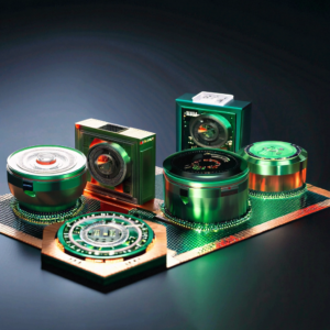
1. Characteristics of BGA
High density: BGA package can provide high density input/output interface, suitable for high pin number chip.
Small size: Because the solder ball is located at the bottom of the chip, the BGA package is more compact than the traditional pin-type package.
Thermal performance: The BGA package can transfer heat directly to the PCB through the solder ball, helping to improve heat dissipation efficiency.
Cost: The initial investment is high, but the cost is relatively low in mass production.
Reliability: BGA package has good vibration and shock resistance.
2. Characteristics of LGA
Easy to replace: LGA encapsulated chips can be directly plugged in and out for easy maintenance and upgrades.
Low cost: no ball welding, reducing the cost of packaging materials.
Thermal performance: Direct contact with the PCB helps to improve heat dissipation efficiency.
Size: The size is between BGA and traditional pin-based packages.
Reliability: Because there is no solder ball, LGA packages may be more vulnerable to physical damage in some cases.
Precautions for selecting the correct packaging method
When considering a BGA or LGA package, there are several key factors to consider to ensure that the package you choose best suits your application needs.
1. Cost effectiveness
BGA: Higher initial cost, but lower unit cost in mass production.
LGA: Material costs are lower, but overall costs may vary as more maintenance and replacement may be required.
2. Space limitation
BGA: Suitable for applications where space is limited, such as smartphones and tablets.
LGA: The size is between BGA and traditional pin-type packages, suitable for applications with slightly less space.
3.I/O density
BGA: Provides a high-density I/O interface for chips with a high pin count.
LGA: The I/O density is relatively low, but still meets the needs of most applications.
4. Thermal Management
BGA: Heat can be transferred directly to the PCB through the welding ball, which helps to improve the heat dissipation efficiency.
LGA: Direct contact with the PCB also helps to improve heat dissipation efficiency.
5. Maintainability
BGA: Once installed on the PCB, it is more difficult to replace.
LGA: The chip can be directly inserted and removed for easy maintenance and upgrade.
6. Reliability
BGA: Good resistance to vibration and shock.
LGA: May be more susceptible to physical damage due to the absence of a solder ball.
7. Application field
BGA: Suitable for high-performance computing, mobile devices, and network devices.
LGA: Suitable for applications that require frequent chip replacement, such as desktop and server motherboards.
8. Design and manufacturing complexity
BGA: The design and manufacturing process is complicated, especially the precise placement of the welding ball.
LGA: The design is relatively simple and the layout of the metal contacts is more flexible.
9. Testing and debugging
BGA: Testing is more difficult because the ball is located at the bottom of the chip.
LGA: Testing is more convenient because the contacts are exposed.
10. Future compatibility
BGA: Custom cooling solutions may be required.
LGA: Easier to adapt to future upgrade needs.
To sum up, choosing the right packaging method needs to consider the above factors. For example, if you are developing a mobile device with high performance and limited space, a BGA package may be the best choice. Conversely, if your application requires frequent chip changes and space is not a major issue, then an LGA package may be more suitable. Understanding these differences and making decisions based on specific application requirements is key to ensuring product success.
Future development trends of BGA and LGA
With the continuous progress of electronic technology, BGA and LGA packaging technology is also constantly developing and evolving. Here are some future trends in these two packaging areas.
1. Higher density
BGA: As chip designs become more complex, BGA packages will continue to evolve toward higher I/O density.
LGA: In order to meet the growing demand for data processing, LGA packages may also adopt a denser contact layout.
2. Smaller size
BGA: New materials and manufacturing techniques will make BGA packages more compact to accommodate the needs of portable electronic devices.
LGA: With the advancement of chip manufacturing technology, LGA packages can also achieve smaller sizes.
3. Cost optimization
BGA: Reduce the initial cost of BGA packaging by improving manufacturing processes and materials science.
LGA: Further reduces costs by improving production efficiency and reducing material waste.
4. Improved reliability
BGA: More advanced packaging technology and stricter quality control will improve the reliability of BGA packages.
LGA: Improved contact design and manufacturing processes will reduce the risk of physical damage.
5. Be environmentally friendly
BGA: Develop environmentally friendly packaging materials to reduce the use of hazardous substances.
LGA: Using sustainable design concepts to improve the recyclability of packaging materials.
6. Intelligent packaging
BGA: Integrates sensors and other intelligent components for package-level monitoring and control.
LGA: Also integrates intelligent functions to improve the overall performance and reliability of the package.
7. Advanced packaging technology
BGA: Explore new technologies such as Fan-Out Package and Wafer Level Package.
LGA: The use of new packaging materials and technologies, such as Hybrid Bonding.
conclusion
Through the in-depth discussion of BGA and LGA, we can clearly see their respective characteristics and application scenarios. With its high density I/O interface and compact design, BGA packages occupy an important position in electronic devices where space is limited and high performance is required. The LGA package, with its ease of replacement and low initial cost, is particularly suitable for applications that require frequent maintenance or upgrades. Choosing the right package depends not only on factors such as cost, space constraints and I/O density, but also on thermal management, maintainability and application areas. With the continuous development of electronic technology, BGA and LGA packaging technology is also improving, towards higher density, smaller size and stronger performance direction.
As your trusted partner, tdt-ele, with its extensive experience and professional technical team, is committed to providing you with tailor-made packaging solutions. Whether BGA or LGA packaging, we can provide the best advice and support for your specific needs to help you stand out in the fierce market competition. If you are looking for a partner who has a deep understanding of your business needs and can provide high-quality packaging services, then we are the best choice. Contact us now!
